Dielectrophoresis (DEP) On a Chip: A Microfluidics Overview
What is Dielectrophoresis (DEP) on a chip?
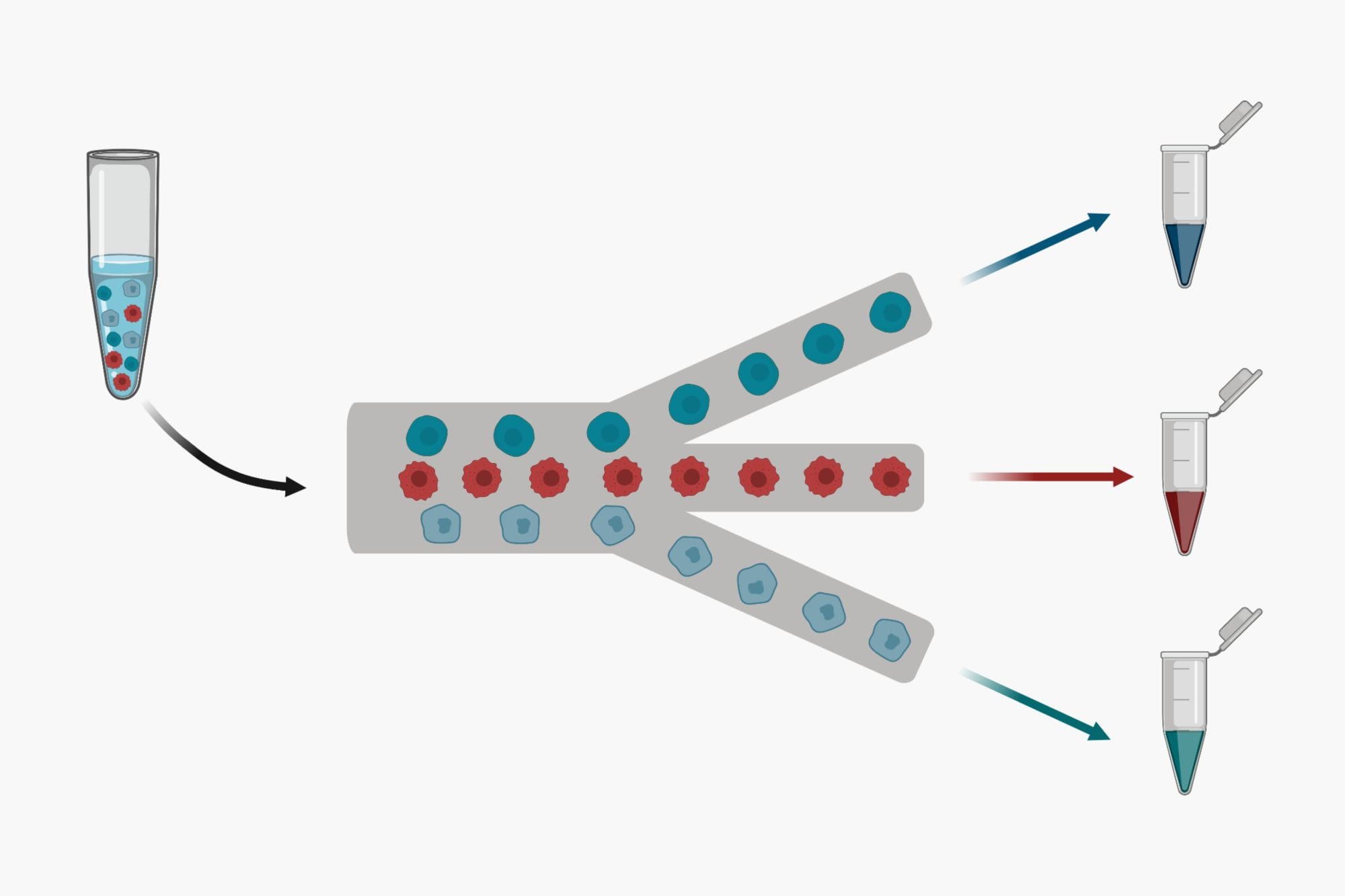
Dielectrophoresis (DEP) effect is the induced motion of polarizable particles in a non-uniform electric field aka E-field. DEP is versatile mechanism to transport, trap, separate and characterize particles such as cells in Microfluidic devices. DEP microfluidic chips aka DEP-on-a-chip are more difficult to fabricate due to need for precise alignment of electrodes with microfluidic channels on the device. Applying effective E-field gradient for bio-particle manipulation usually requires tight alignment between the electrode and microfluidic layers. However, rapid development of microfabrication techniques for microfluidics in the past two decades, has reduced the microfluidics fabrication costs helping with increased entry of DEP-on-chip products to the market. The integration of DEP systems with Microfluidics has enabled inexpensive, fast, highly sensitive, highly selective, and label-free characterization of target bio-particles. This short review provides a practical overview of the DEP theory, its operating strategies, applications on chip, and its current limitations.
How Does Dielectrophoresis work?
DEP Force and CM Factor
DEP refers to the interaction force between a non-uniform E-field and the dipole moment which it induces on a polarizable object. 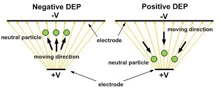 The magnitude of DEP force, FDEP, on a spherical particle strongly depends on permittivity of the medium surrounding the sphere, volume of the bio-particle, gradient of E-field strength, and real-part of Clausius-Mossotti factor, CM*. CM* is a complex variable related to the complex permittivities of the particle and the medium. For a particle more polarizable than the medium, the real part of its CM* factor is positive: Re[CM* (ω)]>0 . This Means the target experiences a positive DEP force, called pDEP, moving it toward the strong E-field region. On the other hand, if Re[CM* (ω)]<0 the particle experiences a negative DEP force, nDEP, and it is moved to the weak E-field region. Figure one illustrates these forces. For a reference with detailed analysis click here.
Two important parameters during design a DEP on chip system to become specific to a target cell trype, are excitation frequency and 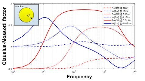 conductivity of the medium. Exerted force on the target cells could be adjusted to be positive, zero, or negative adjusting these parameters. This forms the basis of the separation-on-a-chip platform using DEP. The chart shows how Frequency (ω=2πf ), and the medium’s conductivity (different line types in the image) affect the dielectric signature designated Re[CM* (ω)] and Im[CM* (ω)] curves for a human monocyte.
What are electrode shapes and how they are integrated with Microfluidics in DEP-on-chips?
DEP effectiveness in microfluidic devices heavily relies on the design of E-field pattern and the gradient. Here, we summarize some of the most popular DEP electrode designs for Microfluidics. The E-field gradients, which are essential to induce DEP forces, are 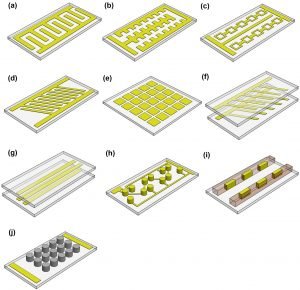 generally generated by two-dimensional (2D), three-dimensional (3D), and insulator-based (iDEP) configuration of electrodes. The 2D electrodes are often patterned within the bottom of the microchannel using conventional lithography techniques, and FDEP is mainly available at the bottom of the microfluidic channels near the electrodes (a-e in this illustration). This 2D strategy causes significant decrease of FDEP in the vertical direction, inversely proportional to the distance from the electrodes. This decreases the throughput due to limited DEP active regions in the bottom of the channel. An alternate approach is using 3D electrode configurations to induce a much stronger DEP response through the entire cross-section area of the channel, forcing the bio-particulate targets more efficiently. The 3D electrodes can be fabricated on the bottom/top surfaces, or sidewalls of the microchannel using more complicated techniques (f-i in the image). Another type of DEP configuration generate spatially non-uniform E-field by using any number of insulating protrusions or obstacles inside the microchannel (insulator-based DEP, or iDEP) without any embedded electrodes, which greatly reduces the complexity of device fabrication (configuration j in the image).
Literature review of DEP on a chip microfluidic devices
With the electrode design (a) in the above image, cell separation based on pDEP and nDEP response can be achieved under optimum excitation frequency and conductivity of cell suspension [2, 3]. S. Shim et al. built up the Re[CM*] lookup spectrum of a wide range of primary mammalian cells for choosing the cross-over frequency fCM during the sorting. Positive-negative DEP sortings were performed, where pDEP responsive cells will be flowing along the flow at the bottom surface near the interdigitated electrodes. On the other hand, cells having nDEP responses were pushed away from the bottom electrode surface and flow along with the carrier fluid at elevated vertical position, called field-flow-fraction(FFF). The castellated electrode patterns shown in (b) are normally used to characterize the cross-over frequency fCM in high throughput[4]. By sweeping the excitation frequency, cells can experience either pDEP or nDEP forces, which attract cells to electrode edges or push cells to the concave areas, correspondingly. By designing an array of ring-shape electrodes (c), cells can be trapped by pDEP or nDEP forces in the electronic cage or physical wells with electrode embedded at the bottom. For nDEP cell trapping, cells can be directly manipulated with regular physiological buffer with high conductivity (~1.5 S/m) under low average flow speed (1 µm/s) to balance the hydrodynamic drag[5, 6]. Oblique interdigitated stripe electrodes are commonly used for nDEP-based cell sorting (d). When cells flow pass each oblique electrode stripe, the net force between DEP force and hydrodynamic drag results in net movement toward the oblique direction to the other side of the microchannel[7, 8].To create arbitrary electrode patterns in real-time, pixelated electrodes (e) were used[9, 10]. Each pixelated electrode pad can be individually controlled on/off to allow the most versatile approach to manipulate individual cells. However, this type of microfluidics devices requires much more complicated microfabrication processes.
In order to create a 3D E-field across the entire cross-sectional area of the device, several electrode designs have been demonstrated. designs (f, g, and h) have the electrode patterns on both top and bottom substrates[11, 12 13, 14, 15,16], which are aligned to form a 3D E-field tunnel, ratchet, or cages to enhance the efficiency of their corresponding 2D electrode designs, for example (d).This type of designs greatly increase the cell processing throughput and can perform operations in high-speed flows. 3D E-field can also be generated by embedding the electrodes along the sidewalls of a microchannel (i) for positive-negative DEP cell separation in high throughput[17, 18].To avoid cells having close contact with electrodes, microscale posts made out of insulators can be arranged to generate local strong E-field area for pDEP manipulations (i) [19, 20]. This methodology is also called insulator-based DEP (iDEP).
Could Current DEP on Chip Designs Be Improved?
The remarkable amount of microfluidics research on DEP has resulted in a variety of different electrode configurations and operation strategies, just to list a few in the discussion above. Despite all achievements in the past, the DEP system can be further improved in many ways, as discussed here:
- The majority of DEP systems require cells to be re-suspended into low conductivity medium (10~100 µS/m) to reduce the Joule heating of sample suspension and risk of electrochemical reaction. Compared to normal physiological buffer with conductivity (1~10 S/m), cells re-suspended in low conductivity medium for a long time may induce negative effect on its physiological functions. Thus, high throughput DEP systems which operate in regular physiological buffer is an active research and commercialization field.
- The assembly of suspended nanomaterials (eq. carbon nanotube) onto the predetermined locations facilitates the creation of novel electronic, optoelectronic and biosensor devices.
- The different DEP elements can be combined in a sequential, flow-through manner to create integrated DEP microfluidic systems capable of handling, concentrating, separating, characterizing of target cells.
References and Further Reading
- Jones, T.B., Electromechanics of Particles. 1995: Cambridge University Press.
- Shim, S., et al., Dielectrophoresis has broad applicability to marker-free isolation of tumor cells from blood by microfluidic systems. Biomicrofluidics, 2013. 7(1).
- Shim, S., et al., Antibody-independent isolation of circulating tumor cells by continuous-flow dielectrophoresis. Biomicrofluidics, 2013. 7(1).
- Morgan, H., M.P. Hughes, and N. G.Green, Separation of Submicron Bioparticles by Dielectrophoresis. Biophysical Journal, 1999. 77(1): p. 516-525.
- Rosenthal, A. and J. Voldman, Dielectrophoretic Traps for Single-Particle Patterning. Biophysical Journal, 2005. 88(3): p. 2193-2205.
- Taff, B.M. and J. Voldman, A Scalable Addressable Positive-Dielectrophoretic Cell-Sorting Array. Analytical Chemistry, 2005. 77(24): p. 7976-7983.
- Han, P., et al., Continuous Label-Free Electronic Discrimination of T Cells by Activation State. ACS Nano, 2020. 14(7): p. 8646-8657.
- Song, H., et al., Continuous-flow sorting of stem cells and differentiation products based on dielectrophoresis. Lab on a Chip, 2015. 15(5): p. 1320-1328.
- Hsu, H.-y., et al., Phototransistor-based optoelectronic tweezers for dynamic cell manipulation in cell culture media. Lab on a Chip, 2010. 10(2): p. 165-172.
- Trapani, M.D., N. Manaresi, and G. Medoro, DEPArray™ system: An automatic image‐based sorter for isolation of pure circulating tumor cells. Cytometry Part A, 2018. 93(12): p. 1260-1266.
- Haandbæk, N., et al., Resonance-enhanced microfluidic impedance cytometer for detection of single bacteria. Lab on a Chip, 2014. 14(17): p. 3313-3324.
- Holmes, D., H. Morgan, and N.G. Green, High throughput particle analysis: combining dielectrophoretic particle focussing with confocal optical detection. Biosensors and Bioelectronics, 2006. 21(8): p. 1621-1630.
- Kung, Y.C., et al., Tunnel Dielectrophoresis for Tunable, Single‐Stream Cell Focusing in Physiological Buffers in High‐Speed Microfluidic Flows. Small, 2016. 12(32): p. 4343-4348.
- Hu, X., et al., Marker-specific sorting of rare cells using dielectrophoresis. Proceedings of the National Academy of Sciences of the United States of America, 2005. 102(44): p. 15757-15761.
- Han, S.-I., Y.-D. Joo, and K.-H. Han, An electrorotation technique for measuring the dielectric properties of cells with simultaneous use of negative quadrupolar dielectrophoresis and electrorotation. Analyst, 2013. 138(5): p. 1529-1537.
- Kelbauskas, L., et al., Optical computed tomography for spatially isotropic four-dimensional imaging of live single cells. Science Advances, 2017. 3(12): p. e1602580.
- Puttaswamy, S.V., et al., Versatile microfluidic platform embedded with sidewall three-dimensional electrodes for cell manipulation. Biomedical Physics & Engineering Express, 2019. 5(5): p. 055003.
- Wang, L., et al., Dielectrophoresis switching with vertical sidewall electrodes for microfluidic flow cytometry. Lab on a Chip, 2007. 7(9): p. 1114-1120.
- Nie, X., et al., High-throughput dielectrophoretic cell sorting assisted by cell sliding on scalable electrode tracks made of conducting-PDMS. Sensors and Actuators B: Chemical, 2021. 327(15): p. 128873.
- Voldman, J., et al., A Microfabrication-Based Dynamic Array Cytometer. Analytical Chemistry, 2002. 74(16): p. 3984-3990.
Learn how microfluidics technology is used to sort and separate cells.
Use electric, magnetic or accoustic forces to sort and separate cells on microfluidic devices.


