Microfluidics Fabrication: Strengths and weaknesses of manufacturing technologies.
There are a handful of technologies currently used to manufacture microfluidic chips. Here we summarize these methods for the fabrication of Microfluidic devices. We would briefly talk about each technology’s shortcomings or strength for the production of Microfluidic platforms.
What is the Size Range in Microfluidics

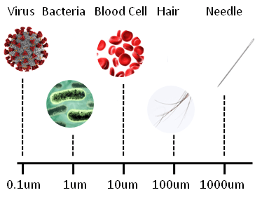
What makes Microfluidic devices distinguishable from others is the presence of small micro features in the device. Feature size is the most important factor in the fabrication of Microfluidics so we describe the size range here. “Small” in Microfluidics means less than 1um to about 1000um. To illustrate, a covid-19 corona virus is about 0.1 um, bacteria is on average about 1um, a red blood cell is just smaller than 10um, a hair could be as thick as 100um, and finally diameter of a needle is about 1000 um, or 1mm.
What is a Microfluidic feature?
A Microfluidic device could be as simple as a hair-thin straight channel inside a microscope slide. In this case, the micro-channel is the feature. Depending on the function of each microfluidic device, the features could be fabricated as a reservoir, well, pillar, wall, cavity, or chamber. In all cases the smallest dimension of these micro features should be in the 1-1000um range to be considered as a microfluidic design. For example a spiral microfluidic channel could be fabricated as long as few centimeters, but the channel width or depth must be less 1mm to fit this definition. It should be noted that size of a part that houses these microfeatures is much greater than the feature size. The size of a microfluidic chip is usually between 1cm-10cm (1/2”-4”).
Why size is important for the fabrication of Microfluidics?
 When it is time to pick a material for the fabrication of microfluidic chips, or narrow down on its microfabrication process or technology, the feature size is the most important factor to consider. Most conventional fabrication processes to manufacture non-Microfluidic devices are not directly applicable in the Microfluidics domain. The first reason is that manufacturing tolerance of the conventional processes is either comparable or larger than the size of the micro-features themselves.
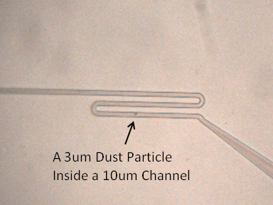
The second main reason is about cleanness of the features of the fabricated microfluidic device. A 3um particle that usually hovers in the air, unnoticed, could easily make a microfluidic device that has a 10um feature non-usable. A similar-size imperfection of the feature could have similar detrimental effect. A manufacturing cleanroom does not mean it is a particle-free environment for microfluidics fabrication. Although cleanrooms do great to isolate outside dust, and remove internal particles via HEPA filters, dust and debris are constantly produced in a high rate due to the manufacturing process itself.
This bring us to the third important reason why size matters in fabrication of microfluidic devices, which is the quality control. Most quality control in Microfluidics must be done under automated microscope for inspection. Depending on the length and population of the micro-features in the device, this could be time-consuming and expensive. Unlike the go-no go gauges used in most industries for checking dimensions and fidelity of parts, there is no way to inspect the micro-features without imaging.
In microfluidics, “smaller” usually translates to “costlier”.
What technologies are used to manufacture microfluidics?
Presently the technologies below are used for the fabrication of Microfluidic parts.  Here we do not intent to have in depth description of each of these technologies, but we give a useful overview of their strength and weakness for the manufacture of parts for microfluidic chips and devices.
Casting
In this method for the fabrication of microfluidics usually a two-part resin is mixed and poured into a mold. Most famous process for casting microfluidic parts is called soft-lithography. A two-part silicone resin called PDMS is poured into molds, cured, and de-molded. PDMS produces the highest fidelity and best quality of micro-features between all manufacturing technologies used for Microfluidics. The feature quality is a replica of the mold without compromise. PDMS features are fully transparent. The biggest drawback of PDMS chips is that PDMS requires time to cure. This makes fabrication cycle too long for large scale production. uFluidix uses proprietary casting methods for high volume production of PDMS microfluidic chips.
Stamping
Stamping aka embossing is usually used for the fabrication of plastic microfluidic parts (as opposed to glass or silicon). Hot embossing is mainly used for thermoplastics such as PMMA, Polycarbonate, or COC. Cold stamping is usually applied to more formable plastics such as PET, Nylon or PP. Hot stamping produces acceptable quality of microfeatures. Micron size features are attainable using this method for microfluidics fabrication. A problem with hot embossing is that the process of embossing is too slow compared to another technology to process thermoplastics called injection molding.
Rolling or Laminating
Rolling is a type of high throughput stamping. It is favored for manufacturing large volume microfluidic chips that are thin, or have forgiving feature structure that would allow for this process. Creating inlet/outlets could be challenging using laminated chips. The laminated microfluidic parts are often used as a component of a larger cartridge.
Micro-Machining
Micromachining may be used for the fabrication of microfluidic devices. In this approach, parts of a block of material such as plastic is removed using rotating tools or laser. Micromachining could be satisfactory for initial trials and prototyping of microfluidic designs, but it is not a manufacturing technology in Microfluidics domain. The main reason is that the fabricated micro-feature’s shape is limited by tool size. In addition, the micro-features would have tool mark resulted from the fabrication process, hence they are not fully transparent. The rough walls could cause issues for the surface to be compatible with specific applications, such as biology or cell studies, and finally micromachining produces dust.
Injection Molding
Injection Molding is normally the first choice when large volume fabrication of microfluidics is needed. The most important thing to remember here is that the features must be designed to be reliably and cheaply produced by injection molding. Injection molding tools are usually expensive in the order of few to tens of thousands of dollars. An improper design could quickly wear the tool down and add to the fabrication cost significantly. For example a complex mold could become a “reject” beyond repair by breaking a few pillars in the mold. There are several other factors here that is outside of the scope of this page.
Etching
Etching means the features are etched out (ie dissolved) using a highly active chemical, often acids, in liquid or vapor form. The etching is usually used for the fabrication of glass or silicon microfluidic chips. First, the parts of the glass or silicon substrate that are not supposed to be etched are covered using a mask. Then the assembly is exposed to the etchant to removed the material for making the micro-feature. The covering masks could be made of photoresists, or any other component that tightly bonds to the substrate depending on the etching method. Most popular etching methods for the fabrication of microfluidic devices are wet etching, DRIE, and RIE. Etching is often the only method available to make glass or silicon chips. It does create satisfactory channels and can be used in low-medium volume. One issue with using glass or silicon for the fabrication of microfluidics is difficulty in making access holes aka ports. Bonding the etched glass or silicon parts to a seal layer is the bottle-neck in this technology and reduces the production rate.
Additive Manufacturing
Additive manufacturing is also known as 3D printing. In this approach the microfluidic device is fabricated layer by layer. There have been many advances in the 3D printing technology recently. Several vendors of 3D printing equipment have reduced their feature resolution. These days, even 10 um feature is available for higher end machines. Although 3D printing has been named one of the candidate technologies for the fabrication of microfluidic chips, there are inherent issues that avoid the technology to be used in Microfluidics. First and most important is that although reduction in resolution helps with fabrication of smaller micro features, it adds to manufacturing time. It is hard to imagine that more than hundred microfluidic parts are manufactured using a single machine in a day. The second is fabrication of cavities. To enclose cavities, microfluidic channels are embedded inside the material, that means there will be leftover resin or sacrificial material that needs to be removed after 3D printing. Complete removal of these materials from the tiny channels in a high volume fabrication setup is a big challenge to the industry. Microfluidics applications, eg biological research, are very sensitive to traces of chemical contamination in the channels. 3D printing technology therefore faces a big issue here. The third problem with 3D printing is about poor optical quality of the 3D printed devices. Many microfluidic systems need near perfect light transmission without distortion which is difficult to achieve with current 3D printed parts in microscale. On the other hand, any 3D print material exhibits enormous autofluorescence if UV light is used for curing the resin. This would hurt applications which need low autoflurescence such as point of care testing cartridges.
The above has been an overview of current industry practice for the fabrication of parts to be used for the manufacture of microfluidic devices. The parts need to be cleaned, and bonded to other components. We will discuss the bonding in a different article.


